Browse categories
Explore
Fiverr Pro
English
$
USD
Need a professional PCB design that is accurate, organized, and ready for manufacturing?
I can help turn your circuit idea, schematic, or existing design into a reliable PCB layout.
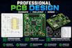
I provide professional PCB schematic design, PCB layout, component placement, routing, BOM preparation, 3D PCB modeling, and fabrication-ready files for electronic projects.
I can work on Arduino boards, microcontroller circuits,
IoT devices, sensors, power supplies, control boards, and other custom electronics.
My workflow focuses on clean routing, proper component placement, design-rule checking, clear labeling, and manufacturing requirements. Depending on your package, you can receive Gerber files, drill files, BOM, pick-and-place files, 3D visualization, and editable source files.
What you get:
Professional PCB layout
Schematic design
Component placement & routing
BOM preparation
DRC/ERC checking
3D PCB visualization
Manufacturing-ready files
Editable source files
Send me your schematic, circuit diagram, component list, or project requirements, and Ill create a professional PCB design tailored to your needs.

File format:
Gerber
•
STEP
•
SCH
•
•
ODB
Software:
Altium Designer
•
Eagle CAD
•
EasyEDA
•
KiCad
•
CircuitMaker
Interface:
HDMI
•
MIPI DSI/CSI
•
USB
•
SPI
•
I2C
•
PCIe
•
Ethernet
Can you design a PCB from my circuit or schematic?
Yes. I can create the PCB layout from your schematic, circuit diagram, component list, or project requirements.
What PCB software do you use?
I can work with professional PCB design workflows and provide editable project/source files depending on the requirements of your project.
Can you provide Gerber files for manufacturing?
Yes. Manufacturing-ready files such as Gerber and drill files can be included according to the selected package.
Can you provide the BOM?
Yes. A Bill of Materials can be provided with component references, values, quantities, and relevant component information.
Can you create a 3D model of my PCB?
Yes. Standard and Premium packages can include a professional 3D PCB visualization.
Can you design multi-layer PCBs?
Yes. I can work on multi-layer PCB designs. The number of layers depends on the package selected and project complexity.
What do you need from me to start?
Please provide your schematic or circuit diagram, component list/BOM if available, board dimensions, connector requirements, and any specific design or manufacturing requirements.
Can you modify an existing PCB design?
Yes. I can update existing PCB layouts, improve routing, modify components, and prepare updated manufacturing files.
Will I receive the source files?
Yes. Editable source files are included according to the selected package.
