Browse categories
Explore
Fiverr Pro
English
$
USD
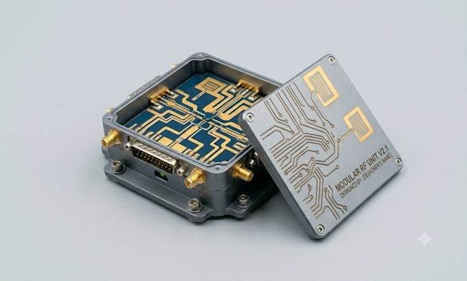
PCB Design Engineer Raspberry Pi, RF PCB, LED PCB, IoT Enclosure Design
You have an RF or microwave idea, but getting it to work reliably in the real world isnt always simple.
Maybe youre struggling with unstable signals, antenna mismatch, or unexpected losses in your PCB.
Maybe your previous design looked fine in simulation but failed during testing.
Or maybe you need a clean RF solution that wont cause issues in manufacturing or deployment.
Thats where this comes in.
You will get RF PCB design, antenna design, RF & microwave circuit design, and PCB layout focused on real performance, so you can move from concept to working hardware with confidence.
What you can expect:
Whether youre building IoT devices, wireless communication systems, or improving an existing RF product, the goal is simple:
Give you a design that works reliably beyond simulation and is ready for real world use.
What do you need from me to start?
Just share whatever you have don’t worry if it’s incomplete. Ideally: Your idea or product description Frequency / application (WiFi, IoT, RF, etc.) Any schematic or rough design (if available) If you’re starting from scratch, I can help you define everything.
Can you work with both new and existing designs?
Yes. I can: Design your RF system from scratch Improve or fix an existing PCB Debug issues like signal loss, antenna mismatch, or unstable performance.
My design works in simulation but fails in real testing. Can you help?
Yes this is very common in RF projects. I focus on real world performance issues like: Signal loss and interference Poor antenna range or mismatch EMI/EMC problems Grounding and layout issues The goal is to make it work in real hardware, not just simulation
Will my design be ready for manufacturing?
Yes. You will receive: Production ready Gerber files BOM (Bill of Materials) PCB stack up details Clean, fabrication friendly layout
What types of RF and antenna designs do you support?
I work on a wide range of RF systems including: WiFi (2.4 GHz / 5 GHz) Bluetooth / BLE LTE / GSM / IoT devices Custom RF and microwave systems Each design is optimized for your exact application.
How do you ensure good RF performance?
I design with real world constraints in mind: Proper impedance matching Low loss PCB layout practices EMI/EMC reduction techniques Careful grounding and shielding Antenna tuning and optimization
What tools do you use?
I work with industry standard tools such as: Altium Designer KiCad RF simulation tools (HFSS / CST / equivalent when required)
How long does a project take?
Typical timelines: Small fixes: 2–4 days RF PCB / antenna design: 5–10 days Full RF system design: 1–3 weeks (Complex projects may take longer depending on scope.)
Can you help if I only have an idea, not a design?
Yes. You can start from just an idea. I can help with: System planning RF architecture Circuit + antenna design Full PCB development
Do you offer revisions?
Yes. I ensure the design meets your expectations: Basic: 1 revision Standard: 2 revisions Premium: multiple revisions for full optimization
