Browse categories
English
$
USD
Connect to your AI
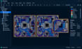
Need a reliable PCB designer to turn your circuit idea into a clean, functional and manufacturing-ready board? Youre in the right place!
I specialize in:
PCB schematic design
PCB layout and routing
Component placement
16 layer PCB design
Gerber and drill files
BOM (Bill of Materials)
3D PCB models
Manufacturing ready files
Source project files
I can work with KiCad, Altium Designer and EasyEDA for electronics, embedded systems, IoT, Arduino, ESP32 and custom PCB projects.
My focus is on accurate schematics, clean routing, proper component placement and reliable manufacturing files. I also perform design checks to help identify common errors before fabrication.
Whether you have an existing schematic or only a circuit idea, I can help turn it into a professional PCB design.
Please send me your project details before ordering so I can recommend the right package for your needs.
Lets turn your idea into a professional PCB!

Will I receive Gerber files and a BOM?
Yes. Depending on your selected package, I can provide Gerber files, drill files, BOM, source files, 3D files, and other required manufacturing documentation.
Which PCB design software do you use?
I work with KiCad, Altium Designer, and EasyEDA, depending on your project requirements and preferred file format.
Can you design multilayer PCBs?
Yes. I can design single, double, and multilayer PCBs. For complex or high density boards, please contact me before ordering so I can review the requirements.
Can you modify or fix an existing PCB design?
Yes. I can review an existing schematic or PCB layout, make requested changes, optimize routing and component placement, and prepare updated manufacturing files.
