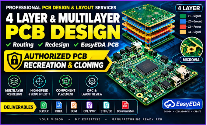
I will design 4 layer multilayer pcb easyeda pcb, redesign pcb boards, gerber files bom

Argentina

I speak English, Italian, Spanish, French

pcb routing, multilayer pcb, gerber files Embedded PCB designs bom Engineer

I’m a PCB design engineer specializing in HDI PCB layout, BGA routing, multilayer PCB design and high-density circuit board layouts. I help startups, electronics engineers, and hardware developers tur...
About this Gig

Hello Valued buyer,


Need a professional 4 layer or multilayer PCB layout, PCB routing, reDesign, or manufacturing ready Gerber files?


I am an Electrical and Electronics DeSigns Engineer specializing in the area of Embedded Systems, Product Desig & Prototyping, Schematics, and PCB layout.


I will design, route, reDesign and optimize your PCB using EasyEDA or other supported PCB tools, based on your project requirements.


Services includes:


  • 4 layer PCB and routing
  • Multilayer PCB layout
  • EasyEDA PCB and layout
  • PCB redesign and layout optimization
  • PCB routing and component placement
  • Power and ground plane PCB
  • High speed and mixed signal routing
  • Differential pair routing when required
  • DRC and layout review
  • Gerber and drill files
  • BOM and Pick and Place files
  • STEP/3D PCB files when required
  • Manufacturing ready PCB documentation
  • Authorized PCB recreation and cloning
  • PCB reverse engineering from suitable customer provided files or references


I can work from schematics, existing PCB source files, Gerbers or other suitable project.


Let's collaborate and bring your electronics visions to life efficiently and effectively. Reach out today to get started on your next innovation!

Specialization:

Circuit design

•

Schematics

•

Layout

•

Footprint

File format:

Gerber

•

STEP

•

VRML

•

Circ

Software:

Altium Designer

•

Eagle CAD

•

EasyEDA

•

Fusion 360

•

KiCad

Interface:

MIPI DSI/CSI

•

I2S

•

SPI

•

I2C

•

PCIe

•

BLE

•

BT

•

GSM/GPRS