Browse categories
Explore
Fiverr Pro
English
$
USD
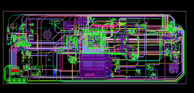
Welcome to professional, enterprise-grade PCB hardware design. If you are looking for a reliable, industry-standard layout engineered using Cadence OrCAD and Allegro, you are in the right place.
I am a hardware design engineer specializing in complex, multi-layer, and high-speed PCB layouts. I deliver production-ready, highly optimized boards designed strictly according to manufacturing tolerances and signal integrity standards.
What I can deliver for your project:
* Multi-layer PCB Layout design up to 6+ layers using OrCAD Allegro
* Professional Schematic Capture & component verification
* High-Speed interface routing (USB, PCIe, Ethernet, CAN, SPI, I2C, UART)
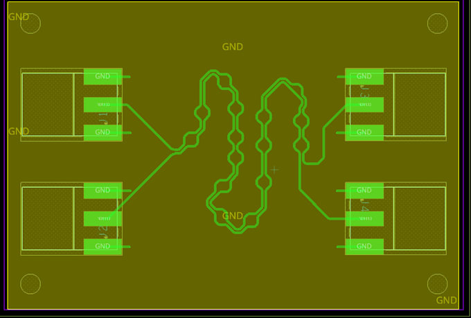
* Length matching, controlled impedance, and noise reduction layouts
* 3D STEP models for mechanical enclosure alignment
* Manufacturing-ready packages: Gerber files, NC Drill, ODB++, and PDF prints
* SMT Assembly files: Bill of Materials (BOM) and Pick-and-Place coordinates
Why work with me?
* Native, clean OrCAD (.DSN) and Allegro (.BRD) source design files
* Strict design rule checking (DRC) for flawless manufacturing
* Clear, transparent engineering support from start to finish
Please message me with your project