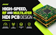
I will design high speed, rf and multilayer hdi pcb layout

United Kingdom

I speak English, Spanish, French, German

PCB Designer and Firmware Development

Electronics Engineer & Embedded Systems Expert specializing in ECG, PPG, SpO2, and wearable medical device development. I design low power, compact and reliable PCB solutions for biosensors, health mo...
About this Gig

High speed and RF boards fail when the layout is guesswork. I design multilayer PCBs where signal integrity, impedance and power delivery are planned from the start.


What I design:

  • DDR3/DDR4, USB, HDMI, PCIe, Ethernet and MIPI interfaces
  • RF and antenna sections (2.4 GHz, sub-GHz, GPS, LoRa, BLE, Wi-Fi)
  • HDI boards with microvias and via-in-pad
  • 4 to 12 layer stackups with controlled impedance
  • Rigid-flex and flex PCB layouts on request


What you receive:

  • Stackup and impedance table for your fab
  • Length matched, differential pair routing
  • Gerber, drill, ODB++ and BOM files
  • Source files in Altium Designer or KiCad
  • Layout notes on EMI and return paths


I use Altium Designer and KiCad, and I follow your manufacturers design rules.


To start, send your schematic, key component datasheets, target layer count and any interface speeds. Not sure it is feasible? Message me and I'll tell you honestly.
Specialization:

Circuit design

•

Schematics

•

Layout

•

Footprint

File format:

Gerber

•

STEP

•

VRML

•

SCH

•

PDF

Software:

Altium Designer

•

Eagle CAD

•

EasyEDA

•

Fusion 360

•

KiCad

Interface:

HDMI

•

I2S

•

TDM

•

UART

•

USB

•

SPI

•

I2C

•

SDIO

•

PCIe

•

Wi-Fi

•

BLE

•

BT

•

GSM/GPRS