Browse categories
Explore
Fiverr Pro
English
$
USD
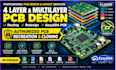
Multilayer PCB Designer, EasyEDA Pro, ESP32, IoT, editable source pcb, fusion360
Need a professional PCB design, schematic, PCB layout, ESP32, STM32, Arduino, IoT, fusion360, Gerber, enclosure design, 4-layer or multilayer PCB for your electronics project?
I will help you turn your schematic, circuit concept or existing PCB layout into carefully organized PCB design using EasyEDA or EasyEDA Pro according to your project requirements.
I specialize in 4-layer PCB layout, multilayer PCB routing, component placement, high-density board layouts and preparation of manufacturing deliverables.
MY SKILLS:
SOFTWARE
EasyEDA, EasyEDA Pro, and compatible PCB design tools as agreed before the project begins.
I focus on clear communication, organized project files, careful layout work, and deliverables that match.