Browse categories
Explore
Fiverr Pro
English
$
USD
PCB Design Expert IoT, Arduino, LED and Embedded Systems
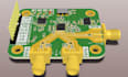
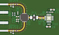
Need a professional RF PCB deslgn for your wireless, IoT, communication, GPS, WiFi, Bluetooth or high-frequency project? You are in the right place!
I specialize in RF PCB design, antenna desgn, RF circuit deslgn, schematic capture, and PCB layout for high-performance electronic products. Whether you are developing a new product or improving an existing deslgn, I will deliver a reliable, manufacturing-ready solution tailored to your requirements.
My services include:
I focus on signal integrity, EMC considerations, optimized routing, and industry best practices to ensure excellent performance and reliability.
Why choose me?
Contact me before placing your order so we can discuss your project requirements and achieve the best results for your RF PCB design project
What information do you need to start my RF PCB project?
I need your project requirements, circuit specifications, operating frequency, PCB dimensions, component preferences, and any reference documents or sketches.
Can you design antennas for WiFi, Bluetooth, GPS, LoRa, and RF applications?
Yes, I can design and integrate antennas for various wireless communication applications, including WiFi, Bluetooth, GPS, LoRa, and other RF systems.
Which PCB design software do you use?
I primarily work with Altium Designer, KiCad, EasyEDA, and other industry-standard PCB design tools.
Do you provide schematics and manufacturing files?
Yes, I provide complete schematic files, PCB layouts, Gerber files, BOM, Pick-and-Place files, and other manufacturing outputs.
Can you redesign or optimize an existing RF PCB?
Absolutely. I can review, troubleshoot, improve, and optimize existing RF PCB designs for better performance and manufacturability.
Do you design multilayer and high-speed RF PCBs?
Yes, I design multilayer PCBs with impedance control, signal integrity considerations, and high-speed routing requirements.
Will you help with component selection and antenna matching?
Yes, I can assist with component selection, RF matching networks, antenna integration, and performance optimization.
Do you offer support after project delivery?
Yes, I provide post-delivery support to help answer questions and resolve any design-related issues within the agreed scope.


