Browse categories
Explore
Fiverr Pro
English
$
USD
PCB and embedded hardware design specialist
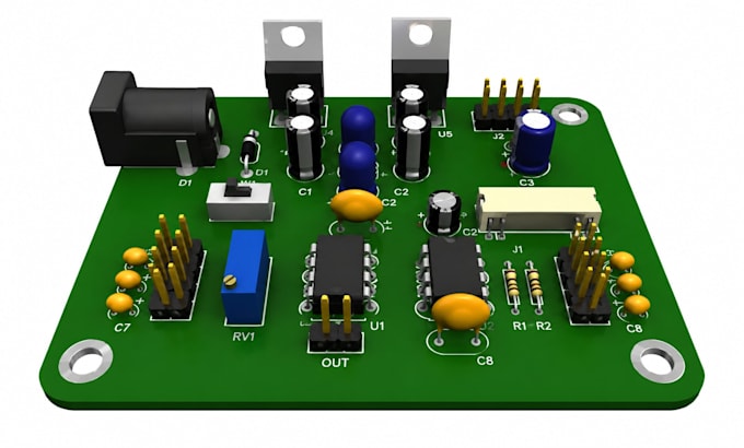
Are you looking for a professional engineer to design an RF PCB, antenna PCB, PCB layout, or reverse engineer an existing PCB using EasyEDA? You've come to the right place!
I'm Obialor Promise, an experienced PCB designer specializing in RF PCB deslgn, antenna deslgn, PCB layout, reverse engineering, and EasyEDA PCB development.
I create reliable, high performance, and manufacturing ready circuit boards for startups, businesses, engineers, researchers, and product developers.
Whether you need a new RF circuit, an optimized PCB layout, or want to recreate an existing board, I deliver accurate designs that meet industry standards.
My Services Include:
Why Choose Me?
Let's turn your idea or existing PCB into a professional, reliable, and fabrication ready deslgn. Contact me today to discuss your project and get started!
What RF PCB design services do you provide?
I offer RF PCB design, antenna design, PCB layout, reverse engineering, EasyEDA PCB design, schematic capture, multilayer PCB layout, BOM creation, and Gerber files ready for manufacturing.
Can you design custom RF and antenna PCBs?
Yes. I design custom RF and antenna PCBs for wireless communication, IoT devices, GPS, Bluetooth, Wi-Fi, LoRa, Zigbee, and other RF applications.
Do you use EasyEDA for PCB design?
Yes. I specialize in EasyEDA and can create professional schematics, PCB layouts, RF designs, and manufacturing-ready files using the platform.
Can you reverse engineer an existing PCB?
Absolutely. I can reverse engineer existing PCBs, recreate schematics, redesign layouts, improve circuit performance, and prepare updated files for manufacturing.
Will I receive all manufacturing files?
Yes. You'll receive EasyEDA source files, Gerber files, BOM, Pick and Place files (if required), PDF schematics, and all files needed for PCB fabrication and assembly.
Can you design multilayer RF PCBs with proper antenna layout?
Yes. I design multilayer RF PCBs with careful component placement, impedance-aware routing, and antenna layout practices to support reliable wireless performance.
What do you need before starting my project?
Please send your project requirements, circuit diagram (if available), preferred RF module or antenna type, PCB dimensions, operating frequency, design constraints, and any reference files. This helps ensure an accurate and efficient design.