Browse categories
English
$
USD
Connect to your AI
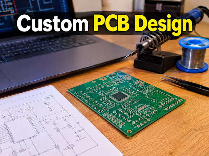
Need a clean and professional PCB design for your electronics project?
I will design your PCB schematic and layout using KiCad or EasyEDA, with organized component placement, routing, and manufacturing-ready files.
What I can provide:
I can work with Arduino, ESP32, sensors, modules, microcontrollers, power circuits, control boards, IoT projects, prototypes, and custom electronics.
You can send me your existing schematic, circuit diagram, datasheet, hand-drawn circuit, or simply explain your project idea. Ill review the requirements and create the PCB design based on your needs.
My focus is on clean layouts, practical routing, organized files, and designs prepared for manufacturing.
Please contact me before ordering if your project has special requirements or a complex circuit. This helps me understand the scope and recommend the right package.
Lets turn your circuit idea into a professional PCB design.


Specialization:
Circuit design
•
Schematics
•
Layout
•
Gerber
File format:
Gerber
•
STEP
•
Software:
EasyEDA
•
Fusion 360
•
KiCad
Interface:
Wi-Fi
What do you need to start my PCB design?
Please provide your circuit schematic, circuit diagram, project requirements, component list, datasheets, or any reference files you have. If you only have an idea, contact me to discuss your project first.
Will I receive Gerber files for PCB manufacturing?
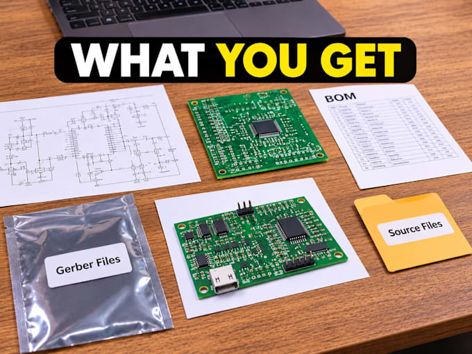
Yes. Gerber files can be included according to your selected package, allowing you to submit your PCB design to a manufacturer.
Can you design custom ESP32 or Arduino PCBs?
Yes. I can design custom PCB layouts for ESP32, Arduino, sensors, modules, microcontrollers, and other electronics projects based on your requirements.
Do you provide the source files?
Yes. Editable project/source files are included according to the selected package.
Can you convert my existing schematic into a PCB layout?
Yes. I can convert your existing schematic into a PCB layout with component placement and routing. Please send your schematic before ordering.
Do you provide BOM and 3D PCB views?
Yes. BOM and 3D PCB views are available according to your selected package.
Can you design a multilayer PCB?
Yes, depending on project complexity and package requirements. Please contact me before ordering multilayer or complex PCB projects.