Browse categories
Explore
Fiverr Pro
English
$
USD
website designer
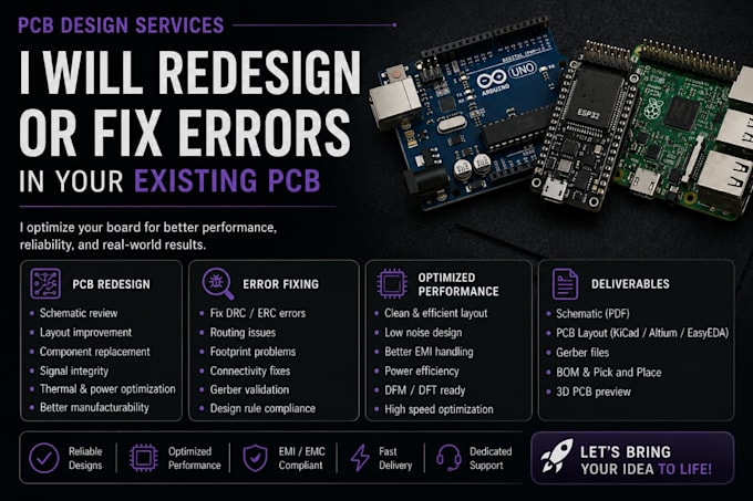
Got a PCB layout with errors, bad signal noise, or manufacturing issues? Lets fix it.
A poorly optimized board can cause unexpected bugs or fail assembly line tests. I will tune up, repair, or completely redesign your current PCB layout to make sure it runs flawlessly and is 100% production-ready.
️ WHAT I FIX:
Layout & Errors: Fixing DRC / ERC errors, tracing routing mistakes, correcting component footprints, and sorting connectivity issues.
Performance Upgrades: Cleaning up layout paths, reducing signal noise, managing heat dissipation, and improving EMI/EMC handling.
WHAT YOU GET:
Full project source files (Altium, KiCad, or EasyEDA)
Clean Schematic layout (PDF format)
Production files (Gerber, NC Drill, BOM, and Pick-and-Place data)
3D board preview model
️ PLEASE NOTE: Every project is unique. To avoid cancelations and save time, please send me a quick message with your project files BEFORE you order so we can pick the perfect package for your design!

Question: What software do you use for PCB layout and redesign?
Answer: I work with industry-standard design tools including Altium Designer, KiCad, and EasyEDA. Please let me know your preferred software when you place your order or send your files.
