Browse categories
Explore
Fiverr Pro
English
$
USD
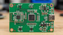
pcb design, embedded system and firmware development
Hello there!
looking for a sleek, efficient, and high performance PCB layout for your electronic project? You're in the right place.
I specialize in designing advanced, compact, and production ready PCB layouts tailored to your device requirements. Whether you're working on a prototype, a commercial product, or upgrading an existing design, I ensure your PCB is optimized for performance, manufacturability, and reliability.
With a deep understanding of modern electronics design principles, I focus on minimizing noise, improving signal integrity, and making the most of limited board space without compromising quality.
What I Will Provide:
Why Choose Me?
CONTACT ME BEFORE PLACING AN ORDER TO DISCUSS MORE ABOUT YOUR PROJECT


_compressed_nxcvfi.jpg)
What do you need to start the PCB design?
I need your schematic (PDF or source file), board size, layer requirements, and any specific design constraints or preferences.
Can you design the schematic as well?
Yes, I can design both schematic and PCB layout. Just send your idea or requirements, and I’ll handle the full design.
Which PCB design software do you use?
I use industry standard tools like Altium Designer, KiCad, and Eagle based on project requirements.
Will the PCB be ready for manufacturing?
Yes, I provide fully DRC checked Gerber files that are ready for fabrication without issues.
Can you design multi layer or complex PCBs?
Yes, I can handle multi layer, high density, and advanced PCB layouts with proper routing and optimization.


