Browse categories
Explore
Fiverr Pro
English
$
USD
ELECTRONIC ENGINEER
Your board, ready for the fab - designed right the first time.
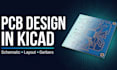
I'm a US-based electronics engineer offering complete KiCad PCB design: schematic capture, component selection, PCB layout, and manufacturing files that pass DRC/ERC clean.
WHAT YOU GET
- Schematic entry in KiCad (from your sketch, datasheet circuit, or existing schematic)
- 2-4 layer PCB layout with proper grounding and decoupling
- Gerber + drill files tested against JLCPCB, PCBWay, OSH Park, or your US fab
- BOM with Digi-Key / Mouser / LCSC part numbers (Standard and up)
- 3D render of your board
- DRC/ERC report with delivery
WHY ME
- Same-time-zone communication and sub-hour responses during US business hours
- NDA-friendly: your design stays yours
- Documentation your manufacturer can actually use
MESSAGE ME FIRST with your schematic, sketch, or idea - I'll confirm scope, timeline, and price before you order. Let's get your board made.

Specialization:
Schematics
•
Layout
•
Gerber
File format:
Gerber
•
BRD
•
SCH
•
•
Circ
Software:
Eagle CAD
•
EasyEDA
•
KiCad
•
Proteus
•
AutoCAD
Interface:
HDMI
•
USB
•
SPI
•
I2C
•
Wi-Fi
•
LTE
•
Ethernet
Will the Gerbers work with my fab house?
Yes, I validate the files against JLCPCB, PCBWay, OSH Park, or any US fab you name before delivery.
Do you sign NDAs?
Yes, on request, before you share anything.
Do I get the KiCad source files?
The Premium package includes the full project; Standard includes Gerbers + BOM; source can be added as an extra.
