Browse categories
Explore
Fiverr Pro
English
$
USD
Hi,
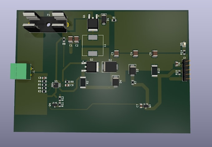
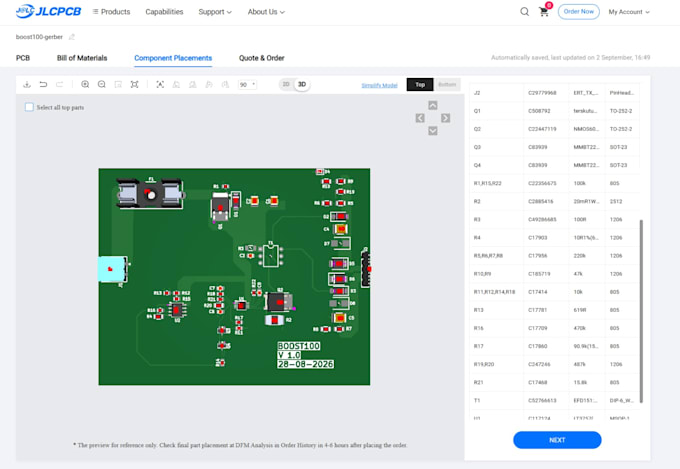
I am an experienced PCB designer with 10+ years of experience in PCB layout, circuit board development, and PCB reverse engineering. I create reliable and professional circuit boards for electronic projects using KiCad, Altium Designer, and EasyEDA.
My services include:
I focus on delivering clean, accurate, and manufacturing-ready layouts based on your project requirements.
Software: KiCad | Altium Designer | EasyEDA
Have a project or an existing PCB that needs improvement? Contact me before placing an order to discuss your requirements. I'll respond as soon as possible.

What information do you need to start a PCB design?
I need your schematic, circuit diagram, component list, PCB dimensions, layer requirements, and any specific design requirements. If you have an existing PCB or reference design, you can provide that as well.
Which PCB design software do you use?
I work with KiCad, Altium Designer, and EasyEDA, depending on your project requirements.
Do you design single-layer and multi-layer PCBs?
Yes. I can design single-layer, double-layer, and multi-layer PCB layouts according to your project requirements.
Do you provide Gerber and manufacturing files?
Yes. I can provide Gerber files and other required manufacturing files so your PCB can be sent to a PCB manufacturer.
Can you reverse engineer an existing PCB?
Yes. I provide PCB reverse engineering services. You can provide clear PCB images, dimensions, component information, or existing files, and I can recreate the PCB design.
Can you modify an existing PCB design?
Yes. I can edit, optimize, and update existing PCB layouts in KiCad, Altium, or EasyEDA.
Can you design complex PCB projects?
Yes. I can work on complex and multi-layer PCB designs. For larger projects or designs with more components, please contact me before placing an order.
Can you design a PCB from my schematic?
Yes. I can convert your schematic into a professional PCB layout, including component placement, routing, and manufacturing files.
Can I contact you before placing an order?
Absolutely. Please contact me with your project requirements before ordering so I can review the project and recommend the appropriate package.