Browse categories
Explore
Fiverr Pro
English
$
USD
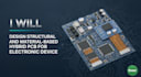
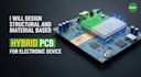
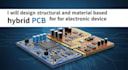
From Idea To Design To Reality
Welcome! Embark on a technological journey with bespoke hybrid PCB designs that seamlessly blend structural integrity and material innovation for your electronic devices.
The Values That I Offered Include:
Custom PCB Layout
Material Analysis
Structural Design
Circuit Simulation
Prototype Testing
Multi-layer Design
Thermal Management
Schematic Capture
Design Optimization
Manufacturing Support
What makes me the best:
Experience paired with innovation ensures the creation of high-performance, reliable PCBs tailored to your specific needs.
Workflow:
1. Send your requirements.
2. Initial analysis and design consultation.
3. Layout and prototype development.
4. Review and revisions.
5. Final delivery and support.
Lets engineer brilliance together ignite your project today with a hybrid PCB design that stands at the frontier of technology. Secure your design consultation and take the first step towards innovation!
What information do you need to start?
A detailed brief about your project requirements, including device specifications and any specific materials you want to use.
Do you provide the final files for manufacturing?
Yes, all necessary files and support are provided to facilitate manufacturing.
Can you assist with material selection for the PCB?
Absolutely, material analysis and selection are integral parts of the service provided.
Are there possibilities for design revisions?
Yes, revisions are included in each package to ensure the final product meets your expectations.


