Browse categories
Explore
Fiverr Pro
English
$
USD
United States
PCB Designer Embedded Systems Engineer Arduino STM32 IoT Expert
Bad pcb layout, noisy signals, and incomplete schematics can delay your prototype and increase manufacturing costs. Many circuit design projects fail because the board is not optimized for production, testing, or real-world performance.
Every revision wastes time, delays delivery, and risks unreliable hardware.
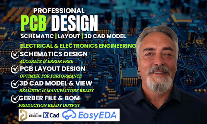
You get professional pcb design, schematic design, electrical engineering, and 3d cad model support built for accurate manufacturing and stable performance. Your circuit board design will be optimized for fabrication, assembly, and testing using Altium Designer, KiCad pcb design, or EasyEDA.
Your delivery includes source files, PDF schematics, Gerber files, BOM, 3D views, and organized project outputs for JLCPCB manufacturing. Fast communication and revision support help your project move from concept



What do you need to start the pcb design project?
You can send your circuit requirements, rough sketch, schematic, BOM, reference images, or existing pcb files. If you only have an idea, the circuit design and schematic development can still be planned from scratch.
Which software is supported for pcb layout and schematic design?
Your project can be completed using Altium Designer, KiCad, EasyEDA, Eagle, Proteus, or Fusion360 depending on your requirements and manufacturing workflow.
Will you provide Gerber files and manufacturing outputs?
Yes. You will receive Gerber files, BOM, pick and place files, PDF schematics, source files, and production-ready outputs compatible with JLCPCB and other manufacturers.
Can you design multilayer pcb and embedded systems?
Yes. Multilayer pcb, ESP32, STM32, Arduino, Raspberry Pi, RF pcb, IoT hardware, and embedded electronic engineering projects are supported.
Do you also create 3D models for pcb and enclosure visualization?
Yes. Your delivery can include 3d cad model files and realistic pcb 3D views for enclosure fitting, presentation, and manufacturing verification.
Can you review or improve an existing pcb design?
Yes. Existing pcb layout, schematic design, routing, grounding, thermal management, and manufacturing issues can be reviewed and optimized for better performance.