Browse categories
Explore
Fiverr Pro
English
$
USD
Lead PCB Designer
I design professional PCBs that actually work. Not just on screen - on the bench.
I'm Parman Josan, R&D Head and Lead PCB Designer at Pelectro with 8+ years delivering high-reliability boards for DRDO defence projects, industrial controllers, medical devices, and consumer electronics.
**What you get:**
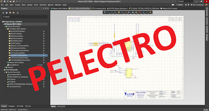
- PCB layout in **Altium Designer** or **KiCad** (2 to 16 layers)
- Controlled-impedance routing for RF, high-speed, and power designs
- 3D collision verification so your board fits before fabrication
- DFM/DFT-compliant Gerber files, BOM, and assembly documentation
- Optional: embedded firmware for PIC, 8051, or Nuvoton MCUs
- Optional: fabrication, assembly, and testing through Pelectro
Real project example:
My Power Driver Card - 13 ICs, dual Molex connectors, through-hole, ultra-compact. Passed 3D verification, manufactured in-house, and worked on first power-up.
I hold a TUV NORD Functional Safety certification (IEC 61508 / IEC 61511) for safety-critical designs.
The screen shows what should work. The bench shows what actually works. That gap is where real engineering lives.
Send me your schematic, requirements, or just an idea. I'll review everything and give you

Can you actually manufacture the board, or just send me files?
I design AND manufacture. I'm R&D Head at Pelectro - we fabricate, assemble, and test boards in-house. You can order just the design files, or the full package: design to a working board on your bench.
I have an idea but no schematic. Can you still help?
Yes. Send me your idea, a hand-drawn sketch, or photos of your current prototype. I'll create the schematic, design the PCB, and guide you through every step. You don't need to be an engineer.
How do I know the board will actually work and not just look good on screen?
Every design goes through 3D collision verification before fabrication. I physically build and test my own designs at Pelectro. The screen shows what should work. The bench shows what actually works.
Do you do safety-critical or industrial designs?
Yes. I hold a TUV NORD Functional Safety Certification (IEC 61508 / IEC 61511) for safety-critical systems. I've designed Zone-0 intrinsically-safe gas detection panels and Ex ia certified circuits for hazardous environments.
Do you handle complex designs like RF and high-speed?
Yes. I've designed 6 GHz communication systems for DRDO, 2.4 GHz RF oscillators, and frequency-hopping secure links. I do controlled-impedance routing, antenna design, and stack-up definition for RF and microwave.
Can you program the microcontroller too, or just design the PCB?
Both. I write embedded firmware for PIC, 8051, and Nuvoton microcontrollers. Order my Premium package for PCB + firmware together. It's cheaper than hiring two separate freelancers.