Browse categories
Explore
Fiverr Pro
English
$
USD
PCB Design, Embedded Firmware, IoT and Wireless Electronics
HELLO AND WECLOME!!
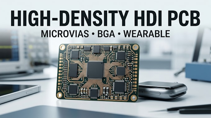
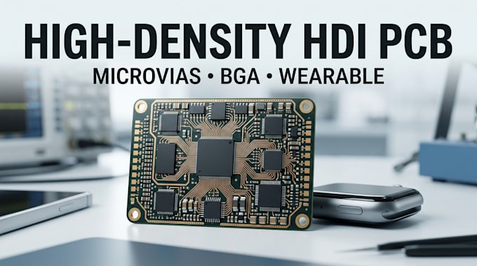
High-Density HDI Wearable PCB Engineering
Smart wearable devices demand compact multilayer boards, dense interconnects, fine-pitch routing, and efficient space utilization. I design high-density HDI PCBs with microvias for smartwatches, smart glasses, fitness devices, IoT wearables, and other miniaturized electronics, with focus on signal integrity, manufacturability, and reliable layout.
What I will provide:
Why Clients Choose Me?
Have a space constrained wearable design? Message me with your requirements and lets develop the right HDI, microvia, and routing strategy.
MESSAGE NOW!!!, THANKS.



Can you route BGA components?
Yes. I can handle BGA escape routing and fine-pitch packages when the selected fabrication process supports the required routing geometry.
Are these PCBs suitable for smartwatches and wearables?
Yes. The layout can be optimized for compact wearable products where board area, component density, and mechanical space are critical.
Can you design microvia structures?
Yes. I can incorporate suitable microvia structures based on the required PCB stackup and your manufacturer's fabrication capabilities.
Do you provide production files?
Yes. Depending on the package, deliverables can include Gerbers, drill files, BOM, pick-and-place files, source PCB files, and technical documentation.
What is an HDI PCB?
HDI means High-Density Interconnect. It uses technologies such as microvias and fine-pitch routing to fit more circuitry into limited PCB space.