Browse categories
Explore
Fiverr Pro
English
$
USD
PCB Design Engineer, PCB Layout and Routing Specialist
Need a custom ESP32 PCB layout for your IoT or electronics project?
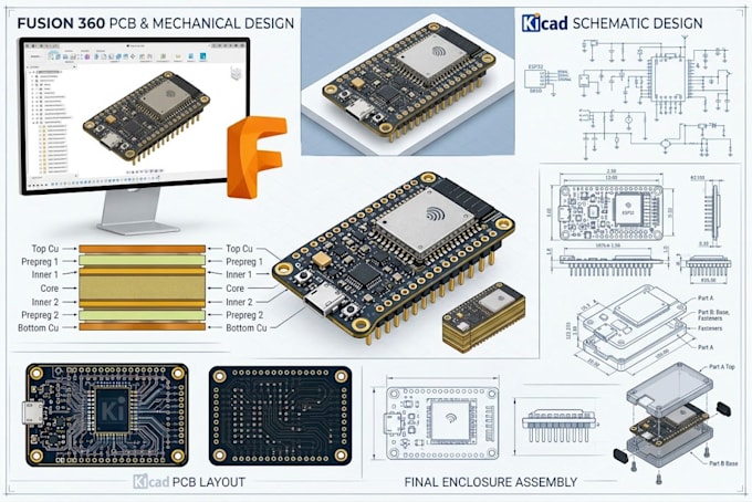
I will design a custom ESP32 PCB layout using KiCad, tailored to your project requirements. Whether you are developing a smart device, an automation system, or an electronics prototype, I can help turn your circuit schematic into a well-organized PCB layout.
My services include:
What you will receive:
Why work with me?
I focus on organized PCB layouts, careful component placement, clear communication, and attention to your design requirements.
To get started, please provide:

What information do you need to start my ESP32 PCB design?
I need your schematic, project description, preferred ESP32 module, component list, and board size if available. If you do not have a schematic, please explain your project requirements before ordering.
Which software do you use?
I use KiCad to create and edit PCB layouts, organize components, route connections, and prepare supported design files.
Will I receive the Gerber files for manufacturing?
Yes, Gerber and drill files are included when specified in your selected package. These files can be submitted to a PCB manufacturer, subject to the manufacturer's requirements.
Can you design a PCB without an existing schematic?
Yes, if your requirements are clear and the required circuit design work is within the agreed project scope. Please contact me first to discuss the project.
Do you provide the physical PCB?
My gig covers PCB design files, not physical manufacturing or delivery of assembled boards. Manufacturing can be arranged separately by you through a PCB fabrication service.
Can you design a 4-layer ESP32 PCB?
Please contact me before ordering. I will review the design requirements and confirm whether the board's layer count and complexity fit the service I can provide.
Do you include revisions?
Yes. Revisions are included according to your selected package. Please ensure your requirements are clear before ordering so I can deliver a design that matches your expectations.