Browse categories
Explore
Fiverr Pro
English
$
USD
Electronics NPI engineer
Looking for a reliable PCB designer to turn your electronic idea into a professional, manufacturing-ready PCB? You're in the right place!
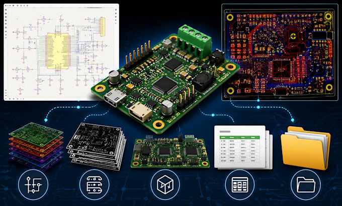
I will design a custom PCB layout and schematic tailored to your electronic product, following industry standard design practices for performance, reliability, and manufacturability. Whether you're developing a prototype, IoT device, embedded system, or commercial product, I can help bring your project to life.
What you'll receive:
Why choose me?
Please contact me before placing an order to discuss your project requirements, complexity, and delivery time. This ensures you receive the best solution at the right package.
Let's build a high quality PCB for your next electronic product!


What information do you need to start my PCB design?
Please provide your project requirements, circuit diagram or schematic (if available), PCB dimensions, preferred software (if any), component list (BOM), and any design constraints. If you're unsure, send me your idea, and I'll help you determine.
What files will I receive after the project is completed?
You'll receive all the files needed for manufacturing and future editing, including schematic files, PCB layout source files, Gerber files, BOM, Pick & Place (if required), 3D PCB model, and PDF documentation.
Can you design PCBs for Arduino, ESP32, STM32, Raspberry Pi, and other microcontrollers?
Yes. I can design custom PCBs for Arduino, ESP32, STM32, Raspberry Pi, ESP8266, and many other microcontroller- and sensor-based projects, depending on your requirements.
Will the PCB be ready for manufacturing?
Absolutely. Every PCB is checked using Design Rule Check (DRC) and is delivered with manufacturing-ready Gerber files that can be sent directly to PCB manufacturers such as JLCPCB, PCBWay, or your preferred fabrication service.
Do you offer revisions if I need changes?
Yes. Revisions are included according to your selected package. If you need additional modifications or feature updates after the project is completed, I'm happy to assist.