Browse categories
Explore
Fiverr Pro
English
$
USD
pcb design
HELLO GREAT BUYER
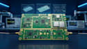
I'm an experienced RF PCB Engineer specializing in radio frequency circuits, wireless communication hardware, and PCB layout. Using Altium Designer, KiCad, EasyEDA, and Eagle CAD, I create efficient, high-performance boards with excellent signal integrity, impedance control, and EMI-conscious routing.
What I Will Provide
Applications
Why Choose Me?
Ready to Get Started?
Whether you need a simple RF module or a complex wireless communication board, I'm here to help. Send me your schematic, specifications, or project idea today, and I'll deliver reliable, fabrication-ready hardware tailored


File format:
Gerber
•
BRD
•
SCH
Software:
Cadence OrCAD
•
Eagle CAD
•
EasyEDA
•
KiCad
Interface:
HDMI
•
BLE
•
BT
•
LTE
What information do you need to start?
Please provide your schematic, operating frequency, PCB dimensions, layer count, BOM, antenna requirements, and project specifications.
Can you design multilayer RF PCBs?
Yes. I design single, double, and multilayer RF PCBs with controlled impedance routing and optimized signal integrity.
Which RF technologies do you support?
Which RF technologies do you support?


