Browse categories
English
$
USD
Connect to your AI
WELCOME!
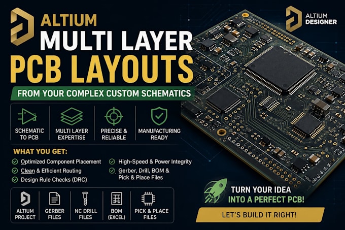
Your schematic deserves more than connected lines it deserves a PCB engineered for real world performance. I transform complex custom schematics into organized, manufacturing ready multilayer PCB layouts using Altium Designer, with precision, clarity, and attention to detail.
Whether you're developing a prototype, upgrading an existing design, or building a complex electronic product, I'll help turn your circuit concept into a practical PCB layout built around your project requirements.
What makes me stand out?
I focus on more than routing tracks. I prioritize component placement, signal flow, board organization, design rule compliance, and manufacturability to help reduce avoidable design issues.
What you can expect:
Deliverables:
Ready to bring your circuit to life? Send me your schematic and project requirements, and let's discuss the best PCB solution for your design.
What do you need from me to start the PCB design?
I'll need your schematic files, project requirements, preferred board dimensions, layer count, component specifications, and any manufacturing constraints. If you have existing Altium files, please share them.
Can you design complex multilayer PCBs in Altium Designer?
Yes! I can help with 2-layer, 4-layer, 6-layer, and higher-layer-count PCB layouts, depending on your circuit complexity and design requirements.
Will I receive the editable Altium source files?
Yes. Your package includes the relevant editable Altium project files, allowing you to review and continue working on your design.
Do you provide manufacturing-ready files?
Yes. Depending on your package, deliverables can include Gerber files, NC drill files, fabrication drawings, and other files required by your PCB manufacturer.
Can you work with my existing schematic?
Absolutely! I can use your existing schematic to develop the PCB layout, subject to file compatibility and schematic completeness.
Do you perform design rule checks (DRC)?
Yes. I perform applicable design rule checks to identify layout violations and address issues within the agreed project scope.
Can you modify or improve an existing PCB layout?
Yes. I can help revise component placement, routing, board organization, and other layout elements based on your requirements.
What if my project is more complex than the listed packages?
No problem! Contact me with your schematic, layer requirements, board dimensions, and project goals. I'll review the scope and recommend a suitable custom offer.