Browse categories
Explore
Fiverr Pro
English
$
USD
PROFESSIONAL PCB DESIGN AND CIRCUIT DEVELOPMENT SERVICES
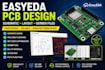
EasyEDA PCB Design for Your Electronics Project
Need an experienced EasyEDA PCB designer to turn your schematic or circuit into a clean, professional circuit board?
Whether you're developing a prototype, IoT device, Arduino project, sensor board, controller, or custom electronics product, I can help transform your design into a properly organized PCB layout prepared for the next stage of manufacturing.
You can get:
I pay attention to board dimensions, component placement, routing, layer requirements, spacing, and manufacturing specifications based on your project requirements.
Already have a schematic? Send it over and I can turn it into an EasyEDA PCB layout.
Before ordering, please provide your project files, board dimensions, layer requirements, and any manufacturer specifications so the project can be reviewed properly.
Let's turn your circuit into a professional EasyEDA PCB design ready for the next stage.

Can you create a PCB layout from my schematic in EasyEDA?
Yes. I can convert your schematic into an EasyEDA PCB layout with component placement, routing, board configuration, and design-rule checking.
Do you work with EasyEDA Standard and EasyEDA Pro?
Yes. I can work with EasyEDA projects depending on the requirements and files provided. Please send your project before ordering if you're unsure about compatibility.
Will I receive the Gerber files for manufacturing?
Yes. Gerber files can be prepared for PCB fabrication according to your selected package and the requirements of your manufacturer.
Can you provide the BOM and Pick & Place files?
Yes. BOM and Pick & Place files can be included where required, depending on the package and the needs of your PCB assembly process.
What do you need before starting my EasyEDA project?
Please provide your schematic or existing EasyEDA project, PCB dimensions, required layer count, component information, manufacturer specifications, and any special design requirements.
