Browse categories
Explore
Fiverr Pro
English
$
USD
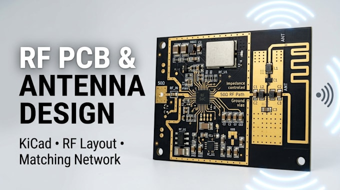
Need a professional RF PCB layout with proper grounding, shielding, and clean routing? Youre in the right place!
I will design high-quality RF PCB layouts optimized for performance, signal integrity, EMI reduction, and manufacturing readiness.
Software Expertise:
Altium Designer (High-Speed & Multi-layer Layouts)
KiCad (Open-Source & Budget-Friendly Projects)
Autodesk Eagle (Standard & Compact Circuit Boards)
What I Can Do For You:
High-Speed Digital & Analog Layouts
Impedance Matching & Signal Integrity Control
RF PCB Design & Antenna Matching Networks
Custom Game Controllers, ESP32, & Raspberry Pi Projects
Rigid-Flex & Multi-Layer Stackups (2 to 12+ layers)
Deliverables Included:
Schematic & PCB Layout Files (Native CAD files)
Manufacturing Files: Gerber, NC Drill, Pick & Place (BOM)
3D Renders of your completed board (STEP/PDF)
With extensive experience in electronics design, I deliver manufacturing-ready circuit boards tailored exactly to your requirements.
Please contact me before placing an order for complex or custom RF PCB projects.
File format:
Gerber
•
STEP
•
SCH
•
Software:
Altium Designer
•
Eagle CAD
•
EasyEDA
•
KiCad
Interface:
UART
•
USB
•
SPI
•
I2C
•
Wi-Fi
•
BLE
•
BT
•
GSM/GPRS
•
LTE
•
Ethernet
What do I need to provide before starting?
Please provide your project requirements, schematic (if available), PCB size, preferred software, component list, and any design specifications.
Do you provide fabrication-ready files?
Yes, I provide manufacturing-ready Gerber files and source files based on your selected package.
Can you redesign or modify an existing PCB?
Yes, I can update, optimize, or modify existing RF PCB layouts and schematics.
Do you design multi-layer RF PCBs?
Yes, I can design 2-layer, 4-layer, and multi-layer RF PCB layouts depending on project complexity.
Which software do you use?
I work with PCB design software depending on project requirements (such as KiCad, Altium Designer, EasyEDA, or Eagle if applicable).
Do you include grounding and shielding optimization?
Yes, proper RF grounding, ground planes, routing, and shielding considerations are included in the design process.
