Browse categories
Explore
Fiverr Pro
English
$
USD
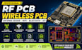
Are you looking for a professional engineer to de sign a reliable RF PCB, wireless communication board, WiFi/Bluetooth circuit, antenna layout, or IoT hardware?
I will provide production-ready PCB des igns optimized for RF performance, signal integrity, impedance control, and wireless connectivity.
Services Included
Contact me before ordering to discuss your project requirements.

What software do you use?
I use Altium Designer, KiCad, EasyEDA, and Eagle CAD depending on project requirements.
Can you design WiFi and Bluetooth PCBs?
Yes. I can design ESP32, ESP8266, Bluetooth Low Energy (BLE), WiFi, GSM, GPS, LoRa, and other wireless communication boards.
Will I receive manufacturing files?
Yes. You will receive Gerber files, BOM, Pick & Place files, and all manufacturing-ready documents.
Can you design PCB antennas?
Yes. I can design PCB antennas, RF matching networks, and optimize antenna placement for wireless performance.
Do you provide firmware development?
Firmware development can be added as an extra service depending on project requirements.
Do I need to contact you before ordering?
Yes. Please contact me first so we can discuss specifications and select the most suitable package.
