Browse categories
Explore
Fiverr Pro
English
$
USD
WELCOME TO MY GIG,
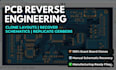
Need to clone a physical circuit board, recreate missing design files, or modernize an obsolete PCB layout? I can help! As an electronics engineering specialist, I provide professional hardware reverse engineering and schematic recovery services using KiCad, Altium Designer, and EasyEDA. I replicate hardware designs from bare board photos, scanner images, or old documentation with 100% accuracy.
What I Offer:
* Complete PCB cloning from high-resolution board photos or scans
* Schematic recovery and manual netlist reconstruction
* Multi-layer layer trace matching and stackup reconstruction
* Component identification and footprint substitution for obsolete ICs
Deliverables Package:
1. Native project files (KiCad or Altium)
2. Production-ready Gerber and Drill files (JLCPCB/PCBWay compliant)
3. Recovered electrical schematic diagram (PDF/SchDoc)
4. Bill of Materials (BOM) with component purchase links
Message me with clear images of your board before ordering.

File format:
Gerber
•
SCH
•
•
ODB
Software:
Allegro
•
Altium Designer
•
EasyEDA
•
KiCad
Interface:
HDMI
•
UART
•
USB
•
I2C
•
BLE
•
BT
•
LTE
•
Ethernet
Can you clone a PCB if some components are burned out or missing?
Yes. By analyzing the remaining track traces and studying the pinouts of adjacent integrated circuits, I can accurately trace the circuit pathways and find direct replacement options for missing parts.
Do you need the physical board shipped to you?
No. Clear, high-resolution smartphone photos or flatbed scanner images of both the top and bottom sides of the bare circuit board are usually all I need to map the tracks accurately.
Will the cloned files work with modern fabrication houses?
Absolutely. I verify all outputs with a strict design rule check (DRC) to ensure the generated Gerber files match standard production guidelines for rapid manufacturing services.
