Browse categories
Explore
Fiverr Pro
English
$
USD
Production Ready PCB Design, Mechanical CAD and Precision 3D Product Modeling
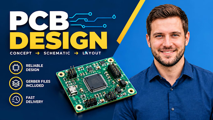
Turn your circuit concept into a clean, reliable PCB engineered for real world use. I'm Sascha Klein, and I provide professional PCB design, PCB schematic, circuit design, and KiCad PCB layout for prototypes, embedded devices, IoT products, and manufacturing.
A good PCB is more than connecting components. Poor component placement, routing conflicts, incorrect footprints, missing documentation, or unresolved DRC issues can delay fabrication and create expensive redesigns. I focus on solving these issues before your board reaches production.
What I can deliver:
You'll receive production ready files such as:
Message me before ordering with your schematic, requirements, or idea so I can confirm the scope and deliverables.
What do you need to start my PCB project?
Please send your schematic or circuit diagram, component list, board dimensions, required interfaces, preferred PCB manufacturer, and any reference files. If you only have an idea or rough sketch, message me and I can help define the requirements.
Can you design a PCB from scratch?
Yes. I can work from a concept, block diagram, circuit requirements, or existing schematic and develop the circuit design, schematic, PCB layout, and manufacturing files.
Do you provide KiCad source files?
Yes. I provide the editable KiCad project files along with the required production outputs, depending on your package and project scope.
Will the PCB be ready for manufacturing?
Yes. I can prepare Gerber, drill, BOM, Pick & Place/CPL, and other manufacturing files, with DRC/ERC and manufacturability checks where applicable. I can also prepare files suitable for manufacturers such as JLCPCB and PCBWay.
Can you design multilayer and high-speed PCBs?
Yes. I can handle single, double, and multilayer PCB layouts, including differential pairs, controlled impedance, USB, SPI, I2C, UART, CAN, RF/Wi-Fi/Bluetooth, and other interfaces based on your requirements.
