Browse categories
Explore
Fiverr Pro
English
$
USD
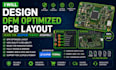
DFM expect and PCB fabrication consultant. I bridge the gap between design and manufacturing, ensuring your boards are produced right the first time with zero factory rejections.
End to end PCB design engineered for seamless fabrication and SMT assembly. I optimize stack ups, clearances, fiducials, panelization, and BOM for JLCPCB/PCBWay standards to save you time and money.
Software;
Altium Designer, KiCad, EasyEDA
What I Offer;
DFM/DFA optimized layout & manufacturer compliant stack up
BOM cross referencing LCSC/Mouser/DigiKey
Fiducial & tooling holes + panelization prep
Full Gerber + BOM + PnP + centroid files
3D model + manufacturing checklist
Why Choose Me;
Zero manufacturing errors guarantee
JLCPCB/PCBWay tested workflows & real time component checks
Fast turnaround & post delivery assembly support
Transparent DFM reporting before final delivery
Stop wasting money on failed prints. Message me with your specs and get a DFM optimized, assembly ready PCB in days!
dfm optimized pcb, jlcpcb ready design, pcbway assembly files, smt pcb layout, bom optimization service, lcsc component check, pcb panelization, fiducial placement, manufacturing checklist.

What does DFM/DFA mean?
Design for Manufacturing/Assembly. I optimize your board to prevent fabrication errors and reduce assembly costs.
Do you verify component stock before finalizing the BOM?
Yes. I cross reference LCSC, Mouser, and DigiKey to ensure all parts are in-stock.
Can you prepare files for SMT assembly?
Absolutely. I generate BOM, Pick & Place, and centroid files formatted for JLCPCB/PCBWay SMT.
Do you handle panelization?
I include panelization guidelines and tooling holes ready for volume production.
What if the manufacturer rejects the files?
I offer free corrections until JLCPCB/PCBWay accepts them without DRC errors.


