Browse categories
Explore
Fiverr Pro
English
$
USD
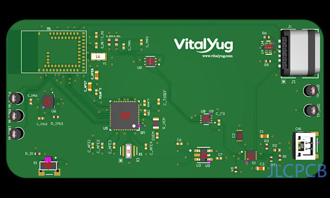
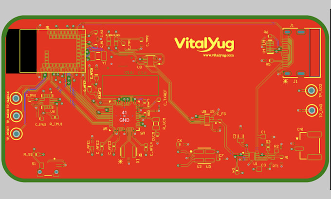
I will design clean, reliable, and manufacturing-ready PCB layouts tailored to your project requirements using Altium Designer and other supported PCB design tools.
My services include:
I focus on organized layouts, appropriate trace widths and clearances, power and ground distribution, and practical manufacturing requirements.
Whether you're developing an embedded electronics project, sensor board, IoT device, or general-purpose electronic circuit, I aim to deliver a well-structured PCB design with clear documentation.
What you can expect: careful attention to detail, transparent communication, and deliverables aligned with the agreed scope.
Please contact me before ordering if your project has complex requirements, unusual components, or specific manufacturing constraints. I'll review your requirements and confirm the scope before starting.


Specialization:
Circuit design
•
Schematics
•
Layout
•
Footprint
•
Gerber
File format:
Gerber
•
SCH
•
•
ODB
•
Pcbdoc
Software:
Altium Designer
•
EasyEDA
Interface:
UART
•
SPI
•
I2C
•
BLE
What do you need from me to start a PCB design?
Share your project idea, circuit requirements, desired features, and board constraints. If you have an existing schematic, component list, or reference design, please share it. If not, I can create the schematic as part of your selected package.
Which PCB design software do you use?
I primarily use Altium Designer. If you require another software format, please contact me before ordering so I can confirm compatibility and the deliverables I can provide.
Will I receive editable source files?
Yes, editable source files are included where specified in your selected package. Depending on the package, deliverables may include native schematic and PCB files, Gerber files, drill files, and a Bill of Materials (BOM).
Do you design multilayer PCBs?
Yes, I offer 2-layer, 4-layer, and 6-layer PCB design packages. Please share your requirements before ordering if your project involves dense routing, specialized interfaces, or other complex constraints.
Are PCB fabrication and assembly included?
Fabrication and physical assembly are not included by default. I provide the design files specified in your package, prepared for the agreed manufacturing requirements. Physical fabrication, assembly, and functional testing must be arranged separately unless explicitly agreed.
Can you prepare files for my preferred PCB manufacturer?
Yes, I can prepare manufacturing outputs according to the manufacturer's supplied specifications and design rules, provided they are within the agreed project scope.
Can you handle complex or specialized PCB projects?
Please contact me first with your project requirements, available files, and design constraints. I'll review the scope and confirm whether I can deliver the requested design before you place an order.