Browse categories
Explore
Fiverr Pro
English
$
USD
Are you looking for a flawless, high-performance PCB layout for your high-speed digital interfaces? Poor routing can lead to signal degradation, EMI issues, and costly board respins. I am here to ensure your hardware works perfectly on the first run.
I specialize in advanced multi-layer PCB layouts using industry-leading tools like Altium Designer and KiCad. I focus heavily on maintaining signal integrity for critical, high-bandwidth communication protocols.
What this gig offers:
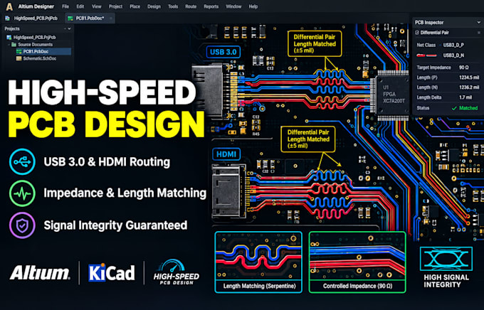
Controlled impedance matching (90Ω for USB, 100Ω for HDMI/Ethernet)
Precise differential pair routing with strict phase/skew control
High-speed length matching and microstrip/stripline optimization
Multi-layer stackup design with dedicated power and ground planes
EMI/EMC mitigation and crosstalk reduction techniques
Production-ready manufacturing files (Gerber, BOM, Centroid)
From USB 3.0 and HDMI to PCIe and MIPI lanes, I bridge the gap between complex schematics and reliable physical hardware. I review your design requirements thoroughly to guarantee robust operation.
Lets secure your signal integrity. Contact me today to discuss your project.
Specialization:
Circuit design
•
Schematics
•
Layout
•
Gerber
File format:
Gerber
•
SCH
•
Software:
Altium Designer
•
Fusion 360
•
KiCad
•
Arduino
Interface:
HDMI
•
I2S
•
I2C
•
BT
