Browse categories
Explore
Fiverr Pro
English
$
USD
Engineering Smarter PCBs for Connected Innovations
Turn your embedded electronics concept into a precisely engineered PCB with dependable USB connectivity and organized KiCad design files.
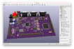
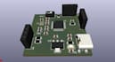
Poor USB routing, unstable power delivery and incorrect component connections can cause failed boards and expensive redesigns. I create embedded PCB layouts, USB circuit schematics and manufacturing documentation using KiCad.
Services Included
Technical Specifications
File Formats
Ready to develop your embedded hardware? Send your circuit requirements or reference files, and let's create a PCB package ready for prototype testing.

Can you design custom USB circuits for embedded systems?
Yes. I design USB-C, USB 2.0, USB-to-UART, and microcontroller USB interfaces using KiCad.
Can you integrate microcontrollers into my USB PCB design?
Yes. I integrate STM32, ESP32, ATmega, PIC, and other MCUs with USB and peripheral circuits.
Can you design USB power management and protection circuits?
Yes. I design USB power regulation, ESD protection, overcurrent protection, and power distribution circuits.
Can you convert my existing circuit schematic into a PCB layout?
Yes. I convert schematics, reference designs, and circuit diagrams into structured KiCad PCB layouts.
Can you design multilayer PCBs with controlled impedance for USB signals?
Yes. I design 2–4 layer PCBs with differential-pair routing, grounding, and impedance requirements.
What files will I receive for PCB manufacturing and assembly?
I provide KiCad source files, Gerbers, drill files, BOM, pick-and-place files, and PCB documentation.


