Browse categories
English
$
USD
Connect to your AI
KiCad PCB Layout and Excel and Google Sheets Trackers
Need a 2-layer board from your finished schematic, or an Eagle/EasyEDA design moved to KiCad? I work in KiCad 9 or 10.
What I offer
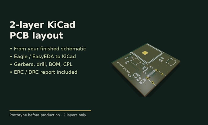
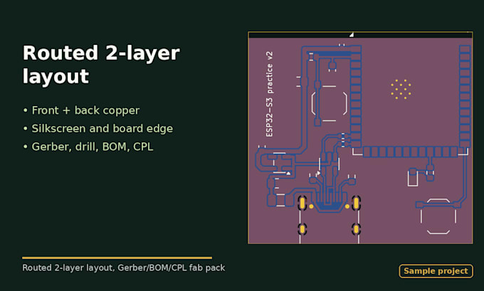
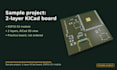
Schematic to routed 2-layer PCB
Eagle/EasyEDA to KiCad conversion, checked against the original
Fab pack: Gerbers, drill, BOM, CPL, 3D view, DRC report
Need a review of an existing board? See my separate PCB review gig.
How it works
1. Message me first with your schematic, board size and fab house
2. I confirm scope, part count and price in writing
3. You get the KiCad project, fab files and a check list
Not offered: mains, RF/antenna or chip-down radio, high-speed routing (USB HS, Ethernet, DDR, HDMI), over 2 layers, circuit design from an idea. Also not offered: Li-ion/LiPo charging or packs (coin cell OK), any rail of 24 V or more, motor drivers, over 3 A on any net.
Delivery starts once schematic, outline and datasheets are complete. Fab files are prepared for upload; you confirm the preview.
I deliver design files to your spec; I can't certify function or compliance (e.g. FCC/CE/UL). Please build and test a prototype before production.
I use AI-assisted tools; every layout is checked by eye and DRC.
Specialization:
Schematics
•
Layout
•
Footprint
•
Gerber
File format:
Gerber
•
STEP
Software:
Eagle CAD
•
EasyEDA
•
KiCad
Interface:
USB
Do I need a finished schematic?
Yes. I lay out and check your circuit; I don't design the circuit itself. A KiCad, Eagle or EasyEDA schematic, or a clear PDF for small boards, is fine. Message me first so I can confirm scope.
Will the board work first time?
No one can promise that. I deliver to your schematic, DRC/ERC clean or every exception explained, footprints checked, but you must build and test a prototype before ordering in volume.
Which fab houses do you support?
Any that accept standard Gerber/Excellon files. I can tune rules and BOM/CPL columns for JLCPCB or PCBWay if you tell me before I start.
What don't you take on?
Mains, RF/antenna or chip-down radio, high-speed routing (USB HS 480 Mb/s, Ethernet), over 2 layers, Li-ion/LiPo charging or packs, rails of 24 V or more, motor drivers, or over 3 A. USB full-speed (12 Mb/s) and pre-certified radio modules are fine.
Do you use AI?
I use AI-assisted tools for checks and file prep; layouts are reviewed by eye and by DRC before delivery. If you'd prefer no AI tools, tell me before ordering.