Browse categories
Explore
Fiverr Pro
English
$
USD
Embedded Systems Engineer, PCB Design and Firmware Developer
I help turn your circuit idea, schematic, or existing design into a manufacturing-ready PCB with the complete files needed for fabrication and assembly.
With 6+ years of experience in PCB and embedded/electronics hardware design, I work with Altium Designer, KiCad, and EasyEDA to develop reliable boards for IoT, industrial, embedded, and electronic products.
What you can get:
The goal is to give you a PCB that is not just designed, but ready to prototype, manufacture, assemble, and move toward production.
Your project information will remain confidential, and NDA support is available if required.
Please contact me before ordering so I can review your requirements and recommend the right package.
Warm regards,
Aizaz
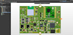

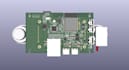
What information do you need before starting my PCB design?
Please provide your schematic or circuit requirements, board dimensions, preferred layer count, component information or datasheets, connectors/interfaces, supply voltages, mechanical constraints and any manufacturer design rules you already have. Reference files are also helpful.
Can you design the PCB if I already have a schematic?
Yes. I can review your existing schematic and create the PCB layout from it. Please send the schematic and any relevant design constraints before ordering so I can confirm the correct package.
Can you create the schematic as part of the project?
Yes, schematic design can be included when the circuit requirements are clearly defined. The required package depends on circuit complexity and component count.
What files will I receive?
Depending on your package and project, deliverables can include Gerber and drill files, BOM, Pick and Place files, PDF schematic/PCB views, editable PCB source files and a 3D PCB model.
Will I receive the editable source files?
Yes. Editable design source files are included in the proposed packages. Please specify whether you require KiCad or Altium Designer files before work begins.
Can you design multilayer or high-speed PCBs?
Yes, multilayer PCB design is covered by the higher packages. Projects involving high-speed interfaces, impedance requirements or unusually dense routing should be discussed before ordering because they may require a custom scope.
Can you create a custom PCB size or shape?
Yes. Please provide the required dimensions, board outline, mounting-hole locations, connector positions and any enclosure/mechanical drawings.
Do you provide manufacturing support?
I can prepare fabrication-ready production files and help resolve reasonable manufacturer questions related to the delivered PCB design. Manufacturing and physical PCB assembly are not included in this PCB-design Gig unless specifically agreed separately.
How do you handle confidentiality and post-delivery support?
Project files and technical information will be handled as confidential project material. If an NDA is required, send it before ordering so its terms can be reviewed. Reasonable questions related to the delivered design can also be addressed after delivery.


