Browse categories
Explore
Fiverr Pro
English
$
USD
HELLO, WELCOME HERE!!
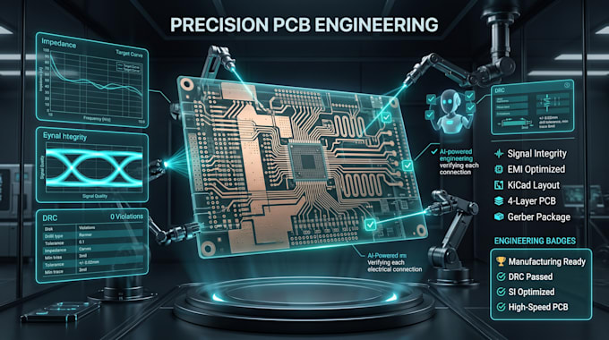
High speed digital PCBs require disciplined routing, controlled signal paths, and manufacturing-aware design practices. I create 4-layer KiCad PCB layouts optimized for embedded systems, high-speed interfaces, industrial controllers, IoT devices, and custom electronics. My workflow emphasizes impedance-aware routing, differential pair matching, return-current continuity, PDN optimization, via transition control, EMI reduction, thermal management, and DFM/DFA validation.
Every design is ERC/DRC verified and delivered with fabrication-ready manufacturing files for reliable prototype and production builds.
What I Offer
Why Choose Me
Let's build a high-performance PCB layout engineered for reliable manufacturing and electrical integrity.


Do you design only in KiCad?
Yes. All PCB layouts are developed in KiCad with editable source files.
Do you support high-speed interfaces?
Yes. I can route USB, Ethernet, CAN, SPI, DDR, LVDS, and other high-speed interfaces.
Are the files ready for fabrication?
Yes. Gerber X2, NC Drill, assembly files, BOM, and manufacturing documentation are included.
Can you design multilayer PCBs?
Yes. I design 2-layer, 4-layer, and higher-layer boards based on project complexity.
Can you optimize an existing PCB layout?
Yes. I improve routing, signal integrity, power distribution, and production readiness.