Browse categories
Explore
Fiverr Pro
English
$
USD
3D ARTIST, BLENDER AND ZBRUSH EXPERT
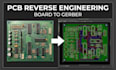
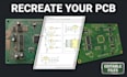
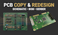
Do you need to reproduce, document, repair or update a discontinued circuit board? I will reverse engineer your PCB from clear photographs, scans, measurements or physical-board documentation and recreate it as an editable schematic and PCB design.
This service is suitable for legacy boards, damaged electronics, unavailable design files, educational documentation and authorized product maintenance.
I can identify visible components, trace accessible connections, redraw the circuit schematic, recreate footprints, rebuild the PCB layout and prepare manufacturing outputs. Deliverables may include schematic source files, PCB layout files, BOM, Gerber files, drill files, PDF documentation and 3D previews.
Accuracy depends heavily on the information provided. High-resolution images of both sides, readable component markings, precise board dimensions and continuity-test results greatly improve the reconstruction.
Only submit boards that you own or have permission to reproduce.
Contact me before ordering so I can inspect the boards complexity and confirm what can be reliably reconstructed.
Can you reverse engineer a PCB using photographs?
Yes, for many visible single-layer and double-layer boards when the photographs are sharp, straight and complete.
Can every multilayer PCB be reconstructed?
No. Hidden internal traces may require X-ray data, destructive analysis, continuity testing or additional documentation.
Can you identify every unknown component?
I can identify readable and commonly available components. Erased codes or proprietary devices may require buyer confirmation or testing.
Will I receive manufacturing files?
Yes, when the available information supports a complete reconstruction and the manufacturing files are included in your package.


