Browse categories
Explore
Fiverr Pro
English
$
USD


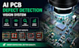
I will build a custom AI-powered visual inspection system for automated PCB defect detection. This solution uses deep learning (computer vision) to identify defects like missing components, solder bridges, wrong parts, scratches, or pad damage in real-time.
What you get:
Defects supported:
The system improves quality control speed and accuracy, reducing manual inspection errors. I can retrain on your specific PCB images for best results.
Perfect for electronics manufacturers, prototyping labs, and automation engineers. Fast delivery, clean code, and documentation included.
Message me before ordering to discuss your PCB types and defect list.
SaaS Onboarding Setup Specialist CRM, Automation Software Integration Expert
Languages
Do I need a GPU to run this?
No, the system can run on CPU for batch inspection. Real-time needs a basic GPU (NVIDIA).
What accuracy can I expect?
95–99% depending on image quality and defect visibility.
Can you detect my specific PCB defects?
Yes. I’ll fine-tune the model using your labeled images for best accuracy.
Is this for production line use?
Yes, can be integrated with cameras, conveyors, or APIs for automation.
