Browse categories
Explore
Fiverr Pro
English
$
USD
PCB specialist
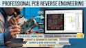
Have a legacy PCB with no documentation, an obsolete circuit board, or a physical sample you need converted into modern digital CAD files? I specialize in professional PCB Reverse Engineering, schematic extraction, and board redesign.
I convert physical circuit boards, high-resolution scans, or damaged samples into production-ready Gerber and CAD files for manufacturing.
What I Provide:
Note: I strictly follow white-hat reverse engineering protocols for legacy support, repair, hardware prototyping, and hardware obsolescence replacement.
Message me clear photos of both sides of your board before placing an order!

Can you reverse engineer multi-layer PCBs?
Yes. For 2-layer boards, clear photos usually suffice. For complex 4+ layer boards, physical inspection or partial de-layering analysis may be required.
What EDA software do you use?
I primarily work in KiCad, Altium Designer, and EasyEDA, depending on your manufacturing or preferred source file needs.
