I will design pcb layout, schematic kicad autocad gerber files bom electronic design

United States

I speak Spanish, English, German, French, Portuguese

Industrial Product Design Engineer CAD PCB Enclosure IoT Automation

I am a Spain-based Product Design Engineer specializing in the development of industrial systems, consumer electronics, IoT hardware, and manufacturing-ready products. I help startups, engineers, and ...
About this Gig

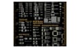
Are you developing an electronic product, IoT device, wearable technology, or industrial system and need a professional PCB design with schematic, layout, BOM, and Gerber files ready for manufacturing?

A successful PCB requires more than routing traces it needs:

  • clean component placement
  • reliable signal and power routing
  • manufacturable board layout
  • thermal and spacing considerations
  • proper documentation for fabrication


This gig is perfect for:

  • PCB design service
  • PCB layout and routing
  • Gerber file generation
  • Altium Designer PCB
  • KiCad PCB layout
  • schematic and BOM design
  • electronics hardware development
  • IoT PCB


WHAT I CAN DESIGN

  • PCB & Circuit Board
  • single-layer PCB
  • double-layer PCB
  • multi-layer PCB
  • compact electronics boards
  • wearable device PCB
  • Schematic
  • analog & digital circuits
  • microcontroller systems
  • sensor integration
  • power management circuits
  • communication modules (WiFi/Bluetooth)
  • Manufacturing Files
  • Gerber files
  • BOM (Bill of Materials)
  • pick-and-place files
  • drill files
  • assembly


I specialize in designing high-quality PCB layouts and schematics for electronics products, ensuring your board is optimized for performance, prototyping, and production.

Specialization:

Circuit design

Schematics

Layout

Footprint

File format:

Gerber

STEP

VRML

BRD

SCH

Software:

Eagle CAD

KiCad

LTspice

NI Multisim

Powersim

PSIM

Interface:

HDMI

MIPI DSI/CSI

I2S

TDM

UART

USB

SPI

SDIO

PCIe

Wi-Fi

BLE

BT

My Portfolio