Browse categories
Explore
Fiverr Pro
English
$
USD
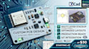
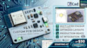
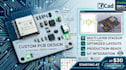
Multilayer PCB High Speed Circuit Design Expert Signal Integrity RF IoT
Stop wasting time and money on broken PCB prototypes.
A single footprint error or bad Gerber file can ruin your production run, delay your product launch, and cause expensive board re-spins.
I deliver error-free, production-ready PCB designs complete with full schematics, verified BOMs, and manufacturing-grade Gerber files designed for seamless fabrication at JLCPCB, PCBWay, or your chosen manufacturer.
What You Get:
Why Work With Me?
Ready to bring your hardware project to life?
Send me your circuit diagram or requirements now to get started.
What files will I receive with my order?
You receive full Gerber files (RS-274X/X2), NC Drill files, Pick and Place (Centroid CPL) files, interactive BOM with part numbers, schematic PDFs, and full source files.
Will my Gerber and BOM files be ready for direct manufacturing?
Yes! All design files follow standard Design For Manufacturing (DFM) rules and are fully compatible with fab houses like JLCPCB, PCBWay, and SeeedStudio.
What software do you use for circuit design and PCB layout?
I primarily work in KiCad and Altium Designer. You will get native source files in your preferred format upon delivery.
What if a component in the BOM is out of stock?
I select components with active stock on Mouser, Digikey, or LCSC. If a part goes out of stock, I will replace it with an identical, easily sourced alternative.
What do I need to provide to start the design?
Simply send your project brief, block diagram, or hand-drawn schematic, along with any specific PCB dimensions or connector placement constraints.


