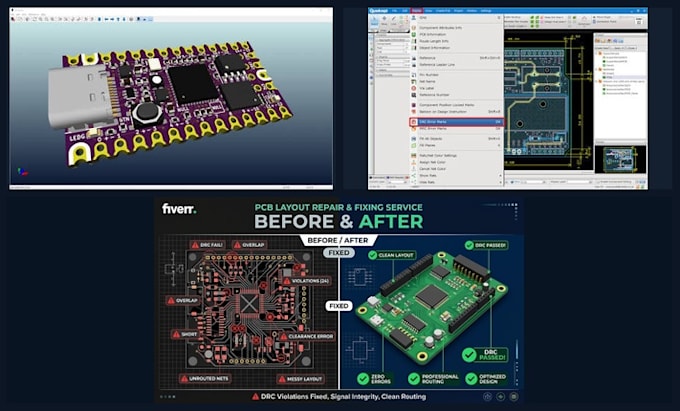
Stuck at JLCPCB checkout due to file errors or failed DFM checks? I will fix your Gerber, BOM, and CPL files so your PCB order gets manufactured smoothly without factory rejections.
Common PCB & JLCPCB Problems I Troubleshoot and Fix:
- JLCPCB Design Rule Check (DRC) failure errors
- Missing, corrupted, or incompatible Gerber files
- Clearance, trace width, and drill size violations
- Unmatched or out-of-stock BOM component part numbers (LCSC)
- Incorrect SMT Pick and Place (CPL/PNP) XY coordinates
- Component orientation, rotation, and alignment errors
- Unconnected nets, short circuits, and ground plane splits
- Missing board outline, keep-out layer, or edge clearance issues
- Silkscreen overlap and illegible component reference designators
- Multi-layer stackup, impedance mismatch, and VIA drill size errors
What You Will Receive:
- Production-ready Gerber files (RS-274X / X2)
- Factory-aligned BOM (Bill of Materials) for SMT assembly
- Correctly oriented Pick and Place CPL files
- Complete DRC verification report & KiCad/EasyEDA source files
Don't let file errors delay your project. Order now for 24-hour fast delivery!