Browse categories
Explore
Fiverr Pro
English
$
USD
Looking to turn your breadboard prototype or electronic schematic into a professional, factory-ready circuit board? You are in the right place!
As an engineering student trained in industrial layout standards, I will design a clean, optimized 2-layer PCB layout for your project using KiCad.
What I will do for you:
-Create a digital schematic trace map from your sketch or image.
-Assign reliable through-hole (THT) or surface-mount (SMD) footprints.
-Route precision copper paths using safe track widths (0.4mm to 1.0mm).
-Apply a full copper ground plane pour to prevent electrical interference.
-Run full Design Rules Checks (DRC) to guarantee a zero-error layout.
What you will receive:
-Factory-ready Gerber & NC Drill files zipped for manufacturing.
-Clear BOM (Bill of Materials) file for part ordering.
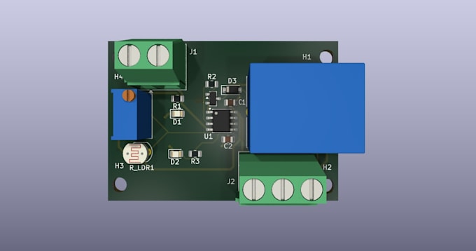
-Photorealistic 3D Renders of your physical board.
Please contact me with your schematic drawing before placing an order so we can select the perfect package for your hardware needs!
Specialization:
Circuit design
•
Schematics
•
Layout
•
Footprint
•
Gerber
File format:
Gerber
•
3DS
Software:
KiCad
Interface:
Wi-Fi
