Browse categories
Explore
Fiverr Pro
English
$
USD
Specializing in KiCad routing schematics and IoT prototyping
Welcome to my professional PCB Design and Layout service!
Are you looking to transform your circuit ideas or schematics into a fully functional, manufacturing-ready PCB layout? You are in the right place. As an Electronic and Communication Engineering (ECE) student with hands-on experience designing PCBs using KiCad, I provide high-quality digital engineering services tailored to your needs.
What I Offer:
Professional Schematic Capture & PCB Layout in KiCad
Single, Double, or Multi-layer (up to 4-6 layers) board design
Optimization for signal integrity and manufacturing constraints (DFM)
Generation of production files (Gerbers, Drill files, BOM, Pick-and-Place)
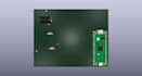
Beautiful 3D models (.STEP format) for enclosure fitting
Why Choose Me?
Dedicated engineering student focused on clean, industry-standard routing
Quick response time and clear technical communication
Affordable pricing for high-quality digital deliverables
Please contact me with your project details before placing an order!




File format:
Gerber
•
STEP
•
VRML
•
SCH
•
Software:
EasyEDA
•
KiCad
•
Arduino
•
Other
Interface:
UART
•
USB
•
SPI
•
I2C
•
Wi-Fi
•
BLE
•
BT
Do you manufacture and ship the physical PCB hardware?
No. I provide the digital engineering and manufacturing-ready files (Gerber files, Drill files, BOM, and 3D models). You can instantly upload these files to rapid-prototyping services like JLCPCB, PCBWay, or OSH Park to get your physical board made cheaply.
Which software do you use for designing the PCBs?
I use KiCad, a powerful open-source EDA software suite. Upon request (in the Premium package or as an extra), I can provide the editable .kicad_pcb and .kicad_sch source files.
What do I need to provide to start the project?
Please provide a clear hand-drawn circuit sketch, a schematic image, a functional description of the circuit, or a specific list of components (datasheets) along with any board size dimensions or constraints you have.


