Browse categories
Explore
Fiverr Pro
English
$
USD
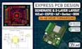
Need a PCB designed fast? I specialize in rapid schematic capture and PCB layout for simple, 2-layer digital and IoT boards using KiCad.
My service is perfect for startups, hobbyists, or engineers who need quick prototyping without sacrificing quality. I focus on clean routing, proper component placement, and strict Design for Manufacturing (DFM) rules.
What I deliver:
Please Note: This gig is designed for fast turnaround of simple/medium complexity boards (up to 20-30 components). I do not handle High-Speed, RF, or complex multi-layer designs in this package.
Please contact me before placing an order to confirm your project requirements!

Specialization:
Circuit design
•
Schematics
•
Layout
•
Footprint
•
Gerber
File format:
Gerber
•
STEP
•
BRD
•
SCH
•
Software:
KiCad
•
Arduino
Interface:
UART
•
SPI
•
I2C
•
Wi-Fi
•
BLE
Do you design high-speed or RF (Radio Frequency) boards?
No, this gig is specifically for simple to medium complexity digital and IoT boards (like ESP32 or relay modules). I do not offer impedance control or RF routing.
