Browse categories
Explore
Fiverr Pro
English
$
USD
PCB Designer, Embedded Hardware Engineer
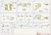
Need a professional PCB designed in KiCad? I can help turn your circuit idea or schematic into a practical PCB design.
I am an Electronics and Communication Engineer with hands-on experience in PCB design, embedded hardware, prototyping, testing and troubleshooting.
What I can help with:
PCB schematic design or modification
PCB layout in KiCad
Component placement and routing
Footprint selection and verification
ESP32 / ESP32-S3 based PCB design
I2C, UART, SPI, USB and sensor interfaces
Power and protection circuits
ERC / DRC checks
BOM preparation
Gerber and manufacturing files
PCB design review and modifications
I focus on practical and manufacturable PCB designs with attention to component selection, routing, grounding, power distribution and reliability.
Please contact me before ordering for complex or multi-layer boards so we can discuss your requirements and scope.

Specialization:
Circuit design
•
Schematics
•
Layout
•
Footprint
•
Gerber
File format:
Gerber
•
STEP
•
VRML
•
SCH
•
Software:
KiCad
Interface:
UART
•
USB
•
SPI
•
I2C
•
Wi-Fi
•
BLE
•
GSM/GPRS
•
LTE
What do you need from me to start the PCB design?
Please provide your circuit schematic, component requirements, board dimensions, connector requirements, layer preference, and any manufacturing requirements you have. If you only have an idea, please contact me first so we can discuss the scope.
Which software do you use?
I primarily use KiCad for schematic capture, PCB layout, component footprints, design checks and manufacturing file preparation.
Can you design an ESP32 PCB?
Yes. I can design PCB circuits based on ESP32 and ESP32-S3 modules, including power, programming, GPIO, sensor and communication interfaces.
Do you provide Gerber and source files?
Yes. Depending on the selected package, I can provide manufacturing files such as Gerbers along with the applicable KiCad source files and documentation.
Can you modify my existing PCB design?
Yes. I can review and modify an existing KiCad schematic or PCB layout based on your requirements. Please share the existing files and required changes before ordering.


