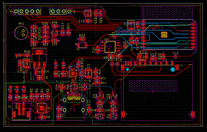
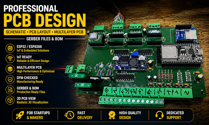
I Wade Nelso, a professional PCB Design Engineer specializing in high-quality PCB layout, schematic design, and multilayer circuit boards using KiCad and industry-standard EDA tools. I work with ESP32, ESP8266, and IoT-based embedded systems, delivering manufacturing-ready designs with Gerber files, BOM, and DFM checks. My focus is on performance, reliability, and cost-effective solutions for startups, makers, and product developers. I ensure clean communication, fast delivery, and client satisfaction.... Read more