Browse categories
Explore
Fiverr Pro
English
$
USD
Need a professional schematic and PCB for your electronic product or prototype?
I am an Electronics Engineer with experience in analogue, digital, low-power and RF hardware. I can help turn your requirements, existing circuit or concept into a practical, manufacturing-ready solution using Altium Designer or KiCad.
Services can include:
Schematic capture and circuit development
Component selection and BOM preparation
PCB layout and routing
Analogue, digital, mixed-signal and low-power electronics
RF-aware and EMC-conscious layout practices where applicable
DFM and manufacturing considerations
Gerber and drill files
Pick and Place files
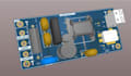
3D PCB views
Schematic and PCB source files
Engineering release summary for suitable projects
I approach each project from an engineering perspective, considering power distribution, grounding, component placement, signal integrity, manufacturability and relevant technical risks.
Please contact me before ordering if your project involves RF, power electronics, high current, complex mixed-signal circuitry or full electronics development so I can review the requirements and recommend the right package.

Specialization:
Circuit design
•
Schematics
•
Layout
•
Footprint
•
Gerber
File format:
Gerber
•
BRD
•
SCH
•
Software:
Altium Designer
•
KiCad
•
LTspice
Interface:
HDMI
•
UART
•
USB
•
SPI
•
I2C
•
SDIO
•
PCIe
•
Wi-Fi
•
BLE
•
GSM/GPRS
•
LTE
Can you work from my idea or requirements?
Yes. I can review your idea, requirements, sketches, block diagrams, or other available information and discuss the most suitable approach. Please contact me before ordering so I can review the project scope and confirm the appropriate package.
Can you create the schematic as well as the PCB?
Yes. Depending on the package and project requirements, I can provide both schematic capture and PCB layout. If you already have a completed schematic, I can also work from your existing files.
What files will I receive?
Depending on the package, deliverables may include: Schematic files and PDF Editable PCB source files Gerber and drill files Bill of Materials (BOM) Pick and Place files 3D PCB views or renders The exact deliverables will be confirmed based on your selected package and project requirements.
Can you work with an existing schematic?
Yes. If you already have a completed schematic, I can use it as the basis for the PCB layout. Please send the relevant files or information before ordering so I can review the scope.
Which PCB software do you use?
I primarily use Altium Designer and KiCad for schematic capture and PCB layout.
Can you help prepare files for manufacturing?
Yes. I can provide manufacturing-ready outputs such as Gerber files, drill files, BOMs, and Pick and Place files, depending on the package and project requirements.
Should I contact you before ordering?
Yes, I strongly recommend it. PCB projects can vary significantly in complexity, even with a similar number of components or layers. Contacting me first allows me to review your requirements, confirm the scope, and make sure you select the most suitable package.


