Browse categories
Explore
Fiverr Pro
English
$
USD
Accurate PCB Design and Hardware Reverse Engineering Solutions
HELLO
And welcome to my gig
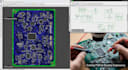
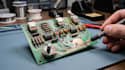
Im a PCB designer and electronics engineer with experience in KiCad-based schematic and PCB design as well as reverse engineering of existing boards.
I work on turning circuit ideas into proper, manufacturable layouts that are clean, functional, and ready for fabrication. This includes schematic design, PCB layout (single and multi-layer), and preparing production files such as Gerber and BOM.
I also handle PCB reverse engineering when you need to recreate or improve an existing board design.
What I Offer
Why Choose Me
Have a circuit or idea? Message me now and lets start building a production-ready PCB for your project.

What do you need to start the project?
I need your circuit idea, schematic (if available), component list, and any size or design requirements.
Can you design without a schematic?
Yes, I can develop the schematic from your idea or reference circuit.
Do you provide manufacturing files?
Yes, I provide Gerber, BOM, and other production ready files.
Can you work on complex or multi layer PCBs?
Yes, I design single, multilayer, and high density PCBs.
Do you offer reverse engineering?
Yes, I can recreate or improve an existing PCB design.
Which software do you use?
I mainly use KiCad for schematic and PCB design.


