Browse categories
Explore
Fiverr Pro
English
$
USD
Your Partner for PCB, Firmware and IoT Solutions
Need a reliable PCB design that is ready to move from concept to manufacturing?
Your circuit deserves more than a basic board layout. You get a structured PCB design focused on clean routing, correct component placement, reliable connections, and manufacturing requirements.
What you get:
Tools & platforms: KiCad, Altium Designer, EasyEDA and industry-standard PCB design workflows.
Whether you need a compact prototype, complex multilayer board, or production-ready PCB, your design is organized for easier fabrication and future revisions.
Send your schematic, circuit requirements, component list, or existing PCB files to get started. Message me before ordering so we can confirm your board requirements and scope.
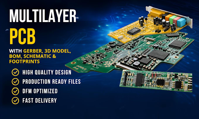
What PCB design files will I receive?
You can receive the schematic, PCB layout, Gerber files, drill files, BOM, footprints, 3D model, and editable source files based on your package.
Can you design multilayer PCBs?
Yes. Multilayer boards can be designed with optimized component placement, routing, layer management, and manufacturing requirements.
Can you create custom footprints?
Yes. Custom footprints can be created and verified according to your component datasheets and PCB requirements.
Which PCB design software do you use?
KiCad, Altium Designer, and EasyEDA are supported depending on your project requirements and source-file needs.
What do you need to start?
Send your schematic, circuit diagram, component list, datasheets, board dimensions, layer requirements, or existing PCB files. If you are starting from scratch, message me to discuss the project.
