Browse categories
Explore
Fiverr Pro
English
$
USD
Power Electronics and PCB Design for Reliable Power Solutions
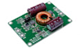
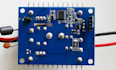
A professional DC-DC converter, buck converter, boost converter, buck-boost converter or power supply PCB for your electronic product, prototype or production project.
I can turn your electrical requirements into a practical and manufacturable power-electronics design with suitable component selection, schematic development, PCB layout and power routing.
MY SERVICES INCLUDE:
DELIVERABLES:
I can work with Altium Designer, KiCad, EasyEDA and other professional PCB design environments.
Please provide your input voltage, output voltage, output current, required power, PCB dimensions and application requirements.
For complex high-voltage or high-current projects, please contact me before ordering so I can review the specifications and confirm the appropriate package.
Can you design buck and boost converters?
Yes, I can design buck, boost and buck-boost converters according to your specifications.
Can you design the PCB too?
Yes. Standard and Premium include complete PCB layout.
Can you select components?
Yes. Component selection can be based on your voltage, current, power and application.
Do you provide Gerber files?
Yes. Gerbers are included in Standard and Premium.
Can you design high-current converters?
Yes, depending on the voltage, current, thermal and mechanical requirements.


