Browse categories
Explore
Fiverr Pro
English
$
USD
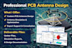
Expert CAD Mold, Automotive PCB Antenna Designer SolidWorks CATIA Altium
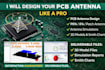
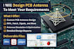
With 8+ years in RF engineering, I design high-performance custom PCB antennas (PIFA, monopole, patch, inverted-F, loop) integrated into your board. Using Altium Designer for layout + Ansys HFSS (or CST) for full EM simulation: impedance matching, S-parameters, radiation patterns, efficiency, gain. Perfect for IoT, Bluetooth, Wi-Fi, GPS, cellular, automotive telematics, or wearables. Deliver tuned layouts, Gerber/BOM, 3D models, simulation reports optimized for compact size, low loss, and certification readiness
What I Offer
Custom PCB trace antenna design (PIFA, monopole, etc.)
RF layout + impedance matching network
Full HFSS simulation (S11, efficiency, patterns)
Gerber files, BOM, assembly drawings
Multilayer PCB integration & optimization
Benefits
Achieve optimal range, gain & efficiency
Reduce prototyping failures & respins
Compact designs fit tight spaces (IoT/automotive)
Simulation reports prove performance pre-build
Manufacturer-ready files speed up production
Why People Choose Me
8+ years RF/PCB expertise with real projects
Proficient in Altium + HFSS for accurate results
Focus on practical, tunable antennas
Fast revisions & clear communication
100% satisfaction
What antenna types do you design?
PIFA, monopole, patch, IFA, loop, dipole – custom for your frequency/band.
Do you provide full simulation?
Yes – HFSS reports with S-parameters, radiation patterns, efficiency (Premium).
What software/tools?
Altium Designer for layout, Ansys HFSS (or CST) for simulation.
What files are delivered?
Gerber, BOM, Drill, 3D STEP, schematic, simulation PDFs, native files.
How long for delivery
Basic: 4–6 days | Standard: 7–10 days | Premium: 10–14 days (rush available).


